Platform: vivado 2017.4
Chip: xc7k325tfbg676-2 (active)
Learning about GTX development. Use the official IP cores provided by xilinx.
Recently after studying the PCIE protocol, using logic to parse the PCIE protocol code various packet headers. Then what is used for data transmission outside? Here is the use of GTX high-speed serial bus. So what is the GTX high-speed serial bus?
We know that general data transfer is done using a parallel bus, a clock line, and a parallel data bus. Data is transmitted on the edge of the clock, and data is transmitted on the double edge of the clock. But the development of parallel transmission always has a great limitation. When the frequency of the clock signal is very high, there are concerns about the clock quality, as well as the stability of the data transmission.
Here with the development of technology, high speed serial buses are slowly being used. High-speed serial buses do not need to transmit a clock signal (the clock signal is extracted from the data, which is then needed to ensure that there are no long consecutive zeros and ones on the serial bus). Compared to parallel data transfer is much more efficient and accurate. Today we will take a look at the high speed serial bus transceiver serdes on xilinx, using an IP core also called (7 Series FPGA GTX/GTH Transceivers) Official information about this IP is available on the UG476.
ug476_7Series_Transceivers.pdf – Viewer – Documentation Portal (xilinx.com)
Xilinx’s 7 series FPGAs have integrated high-speed serial buses. In the FPGA chip is called GTX and GTH, which GTX support rate from 500Mb / s to 12.5Gb / s, and GTH support rate up to 13.1Gb / s. For this rate we come to the conversion to know how fast.
12.5Gb/s=1.5625GB/s=1600MB/s
For many familiar IP protocols are realized through GTX/GTH. For example, PCIE1.1/2.0/3.0, XAUI, Serial RapidIO (SRIO), Serial Digital Interface (SDI) and so on.
catalogs
Uncoded NONE mode example project simulation
Example project simulation using 8B/10B encoding
Example project simulation using 64B/66B encoding
-
GTX Basics
GTX/GTH are integrated on the FPGA and they can be called via IP or proto. Their location in the FPGA is shown below.
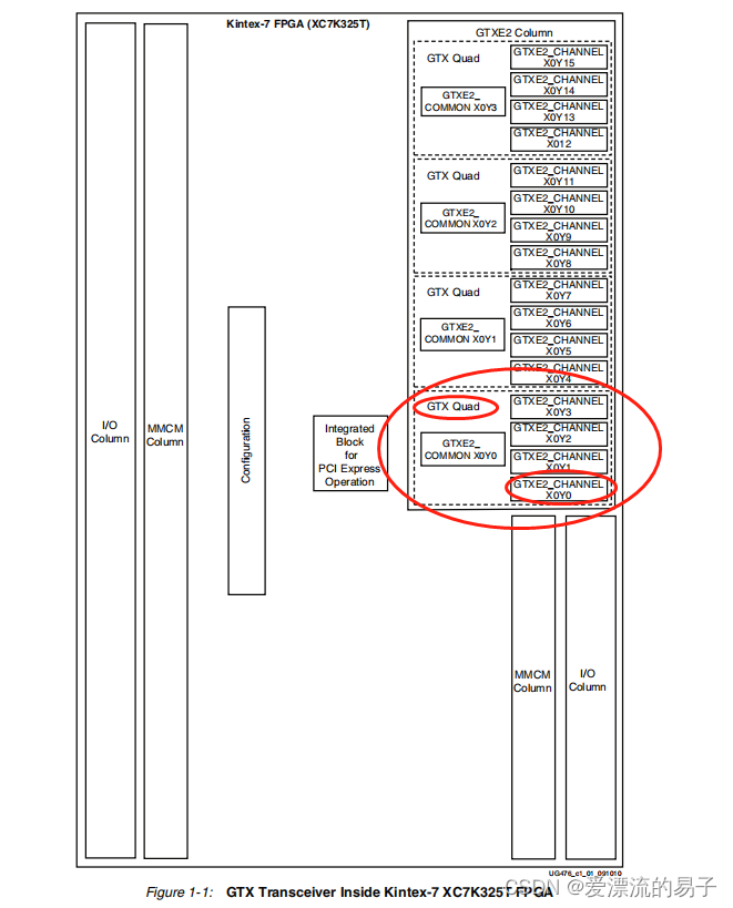
The K7 (XC7K325T) has 16 GTX high-speed transceivers as shown above.
One of the four GTXE2_CHANNEL and one GTXE2_COMMON combined is called Quad or Q. where the GTXE2_COMMON primitive contains a QPLL.
A Quad structure is shown below:
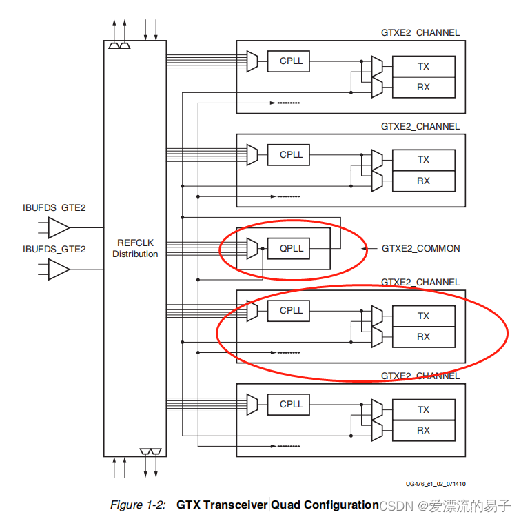
Inside a Quad are four sets of GTXE2_CHANNEL, a QPLL and a pair of differential inputs.
Each GTXE2_CHANNEL contains a set of TXs and RXs, and a CPLL.
CPLL: Inside the GTX, it operates between 1.6GHZ and 3.3GHZ. In GTH, it works between 1.6GHZ and 5.16GHZ.
The operating range of the QPLL is shown in the table below.

The FPGA automatically sets up the QPLL and CPLL according to the requirements of your setup.
A GTXE2_CHANNEL structure is shown below.
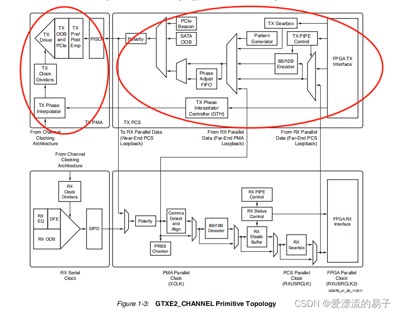
Contains a set of transceivers. For the transmitter TX, he contains a PCS and a PMA. parallel data goes through the FPGA TX interface, passes through the PCS and the PMA, and is then converted into high speed serial data and sent out.
OOB: Out_OF_Band sideband signal.
PISO: Parallel In Serial Out.
| Module (TX) | corresponds English -ity, -ism, -ization |
| FPGA TX Interface | parallel data entry |
| TX 8B/10B Encoder | 8N/10B encoder to encode TX parallel data. Can be bypassed. |
| TX Gearbox | Some high speed data ratespactUse 64B/66B coding.Also support64B/67B code。 |
| TX Buffer | The TX Buffer connects two different clock domains, XCLK and TXUSERCLK, which are contained in the PCS. The TX Buffer is used to match the rates of the two clock domains and to eliminate the phase difference between the two clock domains. |
| TX Buffer Bypass | Bypass the TX buffer. |
| TX Pattern Generator | Pseudo-Random Bit Sequence (PRBS) can be used in GTX to test the BER of high-speed serial channel transmissions. |
| TX Polarity Control | Hardware drawn backwards TX and RX can be used to swap polarity. |
For RX:
EQ : Equalizer/Equalizer;
OOB: Out-Of-Band/Sideband signal;
CDR: Clock and Data Recovery/ Clock recovery.
SIPO: Serial In Parallel Out/Serial In Parallel Out;
| Module (RX) | corresponds English -ity, -ism, -ization |
| RX Equalizer (DFE and LPM) | The RX analog signal comes in and first passes through the RX equalizer, which is mainly used to compensate for the high-frequency loss of the signal during channel transmission.There are two types of adaptive equalizers on the RX receiver side, the LPM and the DFE.The LPM consumes less power, and the DFE can better complement the channel loss. |
| RX CDR | The RX clock data recovery (CDR) circuitry in each GTX_CHANNEL transceiver extracts the recovered clock and data from the incoming data stream. The external data passes through the equalizer first, and then the data coming out of the equalizer goes to the clock data recovery circuitry.The goal of CDR is to find the optimal moment to sample.CDR has a maximum tolerance of concatenated zeros and ones, and if the data is left without a level shift for a long time, CDR loses accuracy. The CDR will lose accuracy if the data is not level shifted for a long period of time, and incorrect sampling will occur. (Therefore we need to use data encoding to reduce the probability of consecutive 0’s and 1’s, serdes supports 8B/10B encoding, 64B/66B encoding) |
| RX Polarity Control | Hardware drawn backwards TX and RX can be used to swap polarity. |
| RX Pattern Checker | Built-in PRBS checker that works before boundary alignment and decoding, this feature can be used to test the integrity of the signal. |
| RX Byte and Word Alignment | Serial data must be boundary aligned to be used as parallel data. This boundary is an identifiable sequence, often called a comma, sent by the TX. the receiving end finds this comma in the data and parallelizes the data that follows it using this identifier as the boundary. |
| RX 8B/10B Decoder | 8B/10B decoder. |
| RX Buffer Bypass | Adjust the phase difference to realize reliable data transfer. It mainly solves the phase difference between the SPIO parallel clock domain to the PCS RX XCLK to realize reliable data transmission between SPIO and PCS. |
| RX Elastic Buffer | GTX/GTHThe transceiver includes two internal parallel clock domains: the PMA parallel clock domain XCLK and the RXUSRCLK clock domain. In order to receive data correctly, the PMA parallel rate must match the RXUSRCLK clock rate and resolve cross-clock domain issues. |
| RX Buffer Bypass | Bypassing the RX resiliency buffer is an advanced feature of the Series 7 GTP transceivers.The RX phase alignment circuit is used to adjust the phase difference between the SIPO parallel clock and the XCLK clock domain to ensure reliable data transfer from the SIPO to the PCS components. |
| RX Clock Correction | The RX Elastic Buffer area is used to connect two different clock domains, RXUSERCLK and XCLK. even if these two clocks are of the same frequency, there are some differences, which require clock corrections. To make the correction, the GTX periodically transmits special characters and allows the GTX/GTH to remove them from the elastic buffer. Receiver overflow and underflow are prevented. |
| RX Channel Bonding | Protocols such as XAUI and PCIE use multiple serial transceivers to produce higher data throughput. Since each transceiver is on a different channel with different latencies, this can lead to “misalignment” of data between channels, which is solved by the RX channel bonding feature. The RX channel binding function solves this problem. The transmitter sends some special characters. The receiver receives them, judges the offset between each channel, and adjusts it. Only 8B/10B encoding is supported. |
-
Use of IP
The first bunch of basics is all about xilinx’s introduction to their products on the UG476. Here we start to configure an IP and do a simple send/receive test on it.
First search the IP catalog for GT
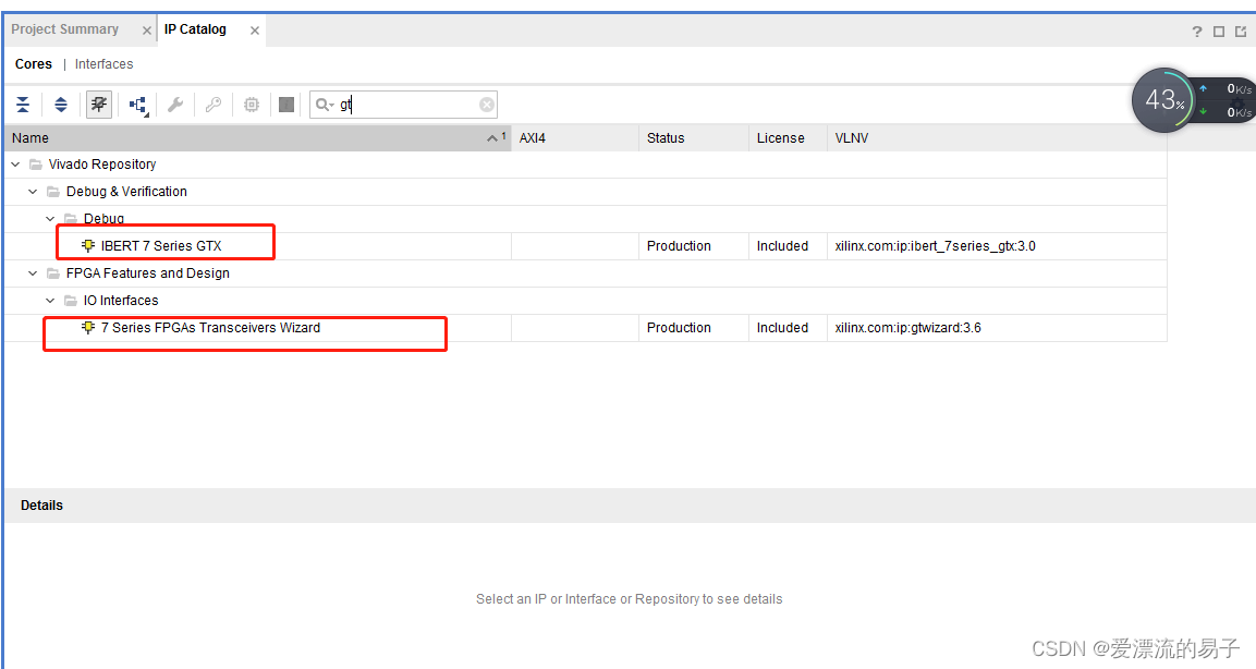
The following two IPs appear.
IBERT 7 Series GTX is testing the quality of the GTX transmission channel.
The 7 Series FPGA Transceivers Wizard is the subject of our test today.
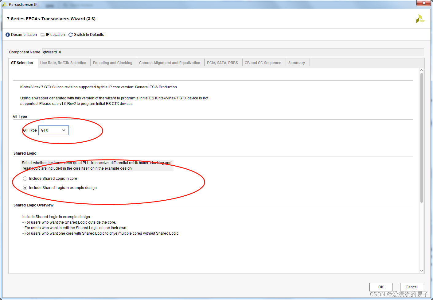
The first page defaults just fine, the chip we use is xc7k325tfbg676-2 (active) defaults to GTX.
The next second page of configuration is more important.
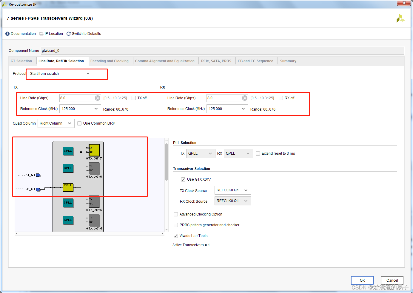
Here serdes supports many kinds of protocols, we directly choose start form scratch (no protocol).
Next, configure the line speed, we are using a GTX, which can range from 0.5Gbps to 10.3125Gbps.
Here the line speed range interval can be selected, the software will be based on the rate you choose to automatically calculate a good range of reference clock. Here we choose 8Gbps, the serial clock reduced by CDR is 4GHZ, and the reference clock calculated by the software is 125MHZ (more common). As we mentioned earlier, CPLL and QPLL support different line rate reference ranges. Here we set the line rate to 8Gpbs, which is already beyond the frequency range supported by the GTX’s CPLL (CPLL ranges from 1.6GHZ to 3.3GHZ).
The next step was to choose which transceiver to use, looking at the UG476 Appendix GTX Transceiver Package Placement Diagrams. in conjunction with the hardware schematic, we found that the GTX_X0Y7 transceiver was used. We have selected the transceiver located on Quad on BANK116. Only one set is selected here.
Check VIVADO LAB TOOLS, you can easily open XILINX example project.
Next, page three. Configuring Coding and Clocking.
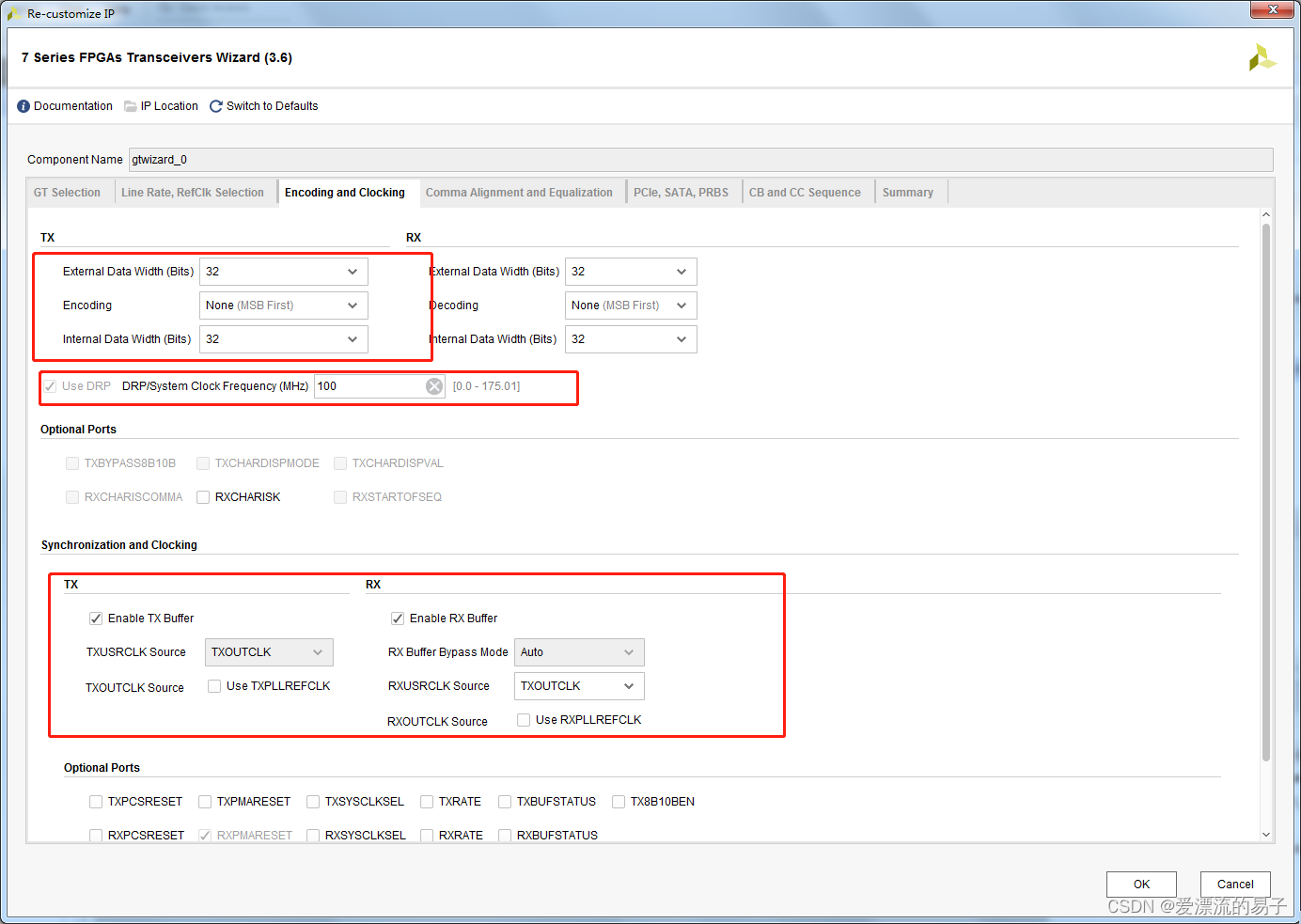
Select the data bit width. The externally supported data bit width, here the default is 32 bits.
Coding method.
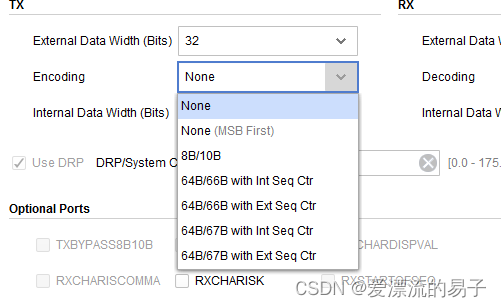
Many types of encoding are supported here.
None No coding. Data is sent directly, in LSB and MSB first.
8B/10B coding.
64B/66B encoding. Divided into two counter modes.
64B/67B codes. 64B/66B, 64B/67B both use theGearboxHigh-speed coding protocols.
Next up is the Configure Boundary Alignment and Equalizer settings on page four.
The no encoding mode we chose first, just default it directly. For 8B/10B encoding in the configuration.
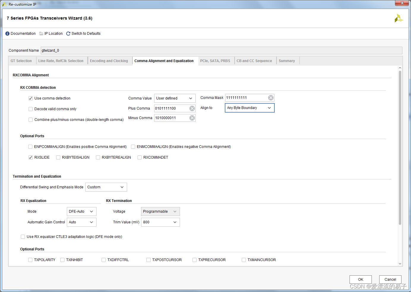
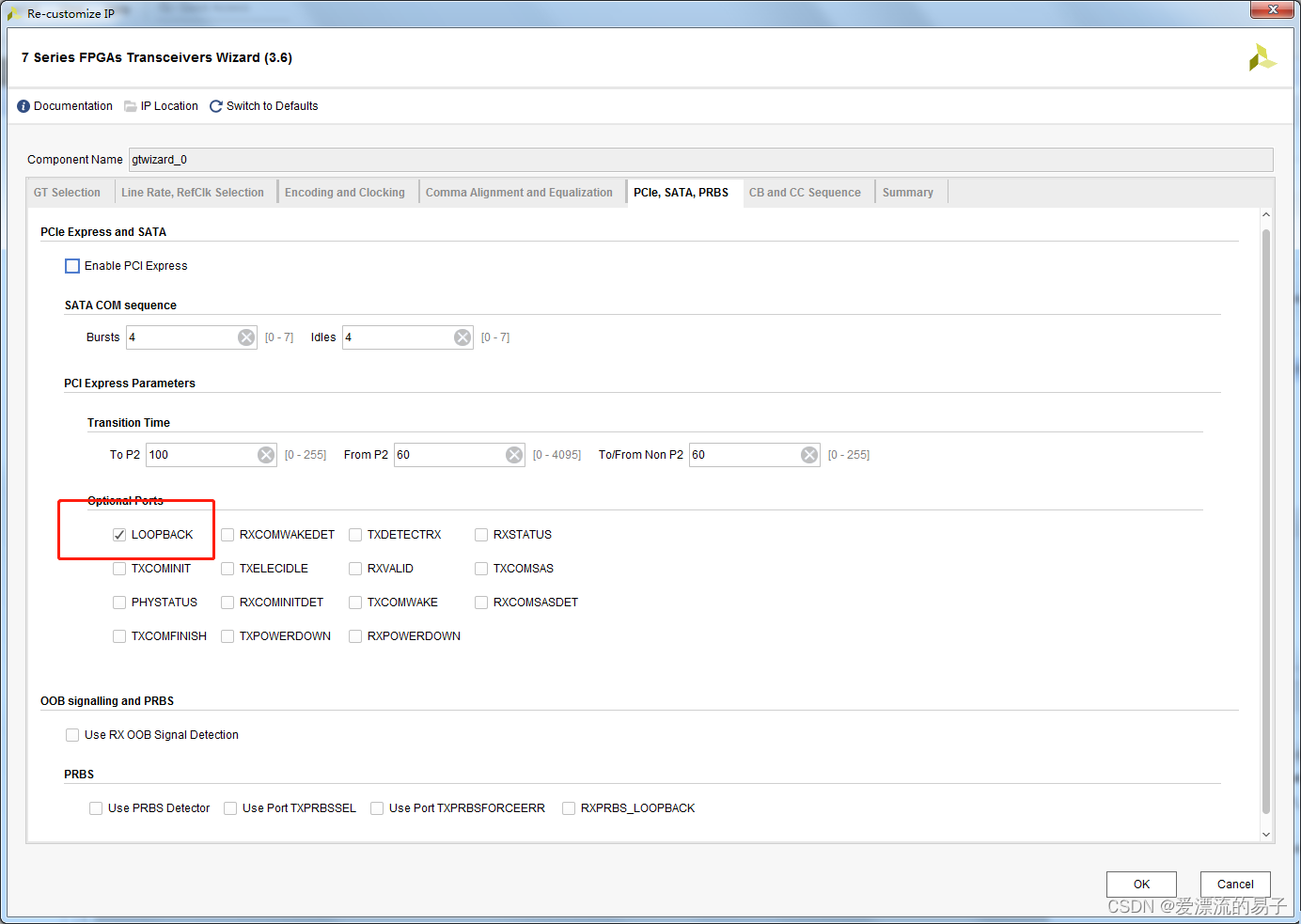
The configuration on page 5, the PCIE part is not set. The LOOPBACK loopback is suspended.
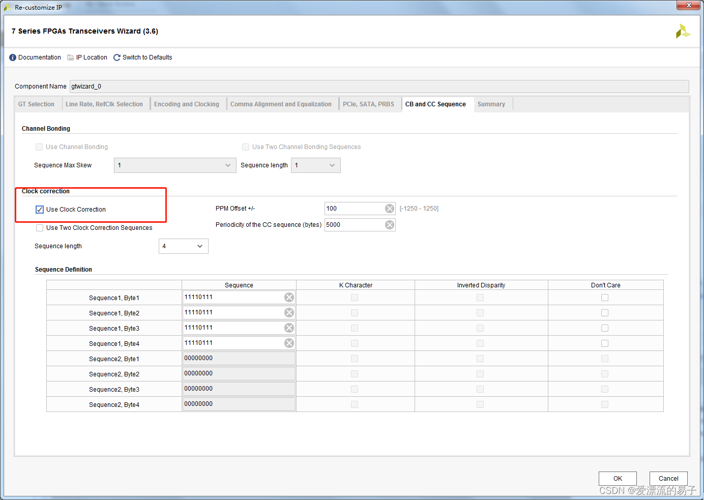
Page 6 Configuring Clock Calibration Defaults on page 6 is sufficient.
Page 7 Summary
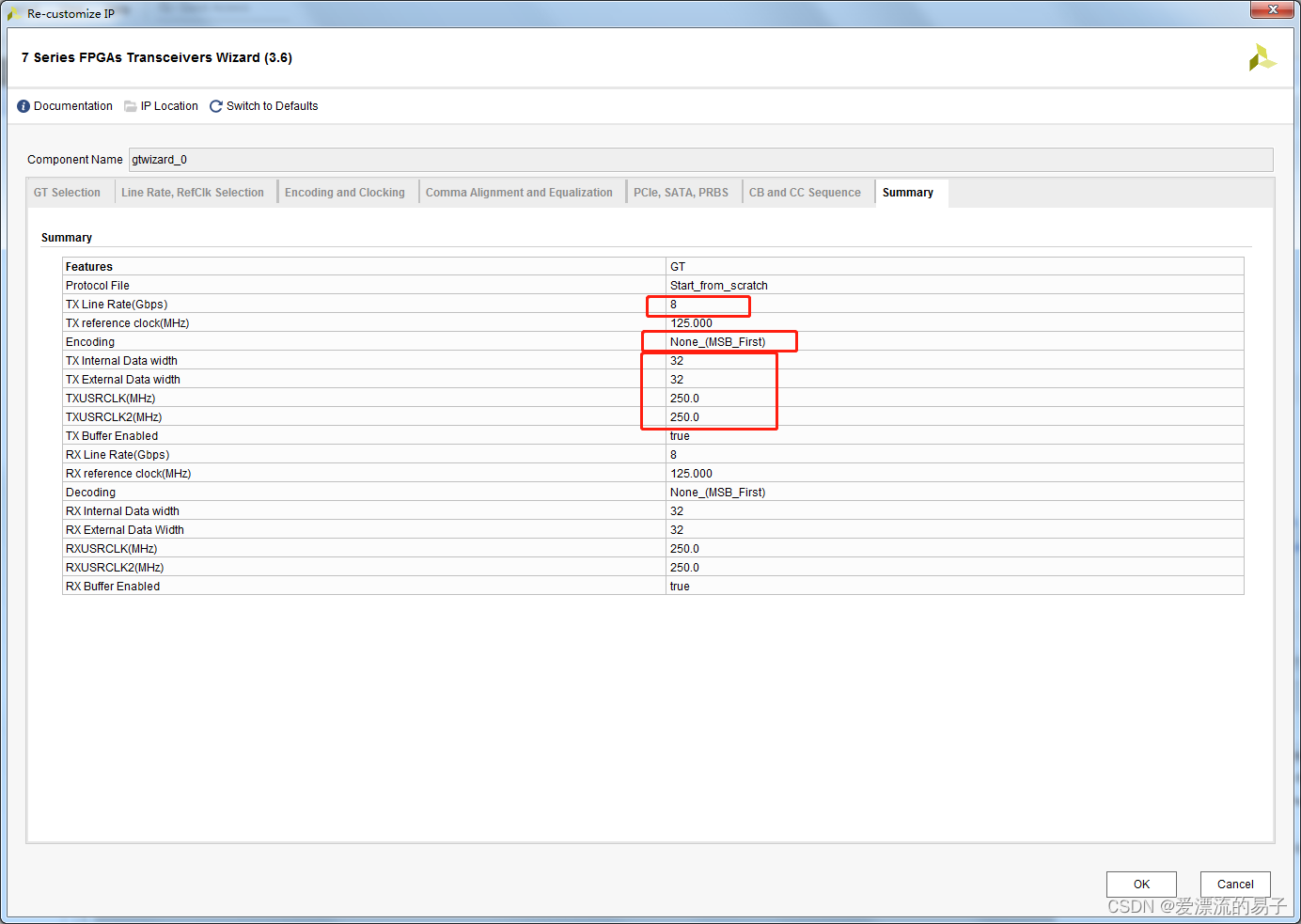
Line rate 8Gbps, data bits 32 bits, TXUSRCLK 25MHZ, coding mode uncoded high bit first.
Next, we’ll open the example project
-
Uncoded NONE mode example project simulation
Mode 1: 8Gbps rate, no coding mode, 32-bit data bit width. rx reference clock 125MHZ.
Open the example project with the following code structure.
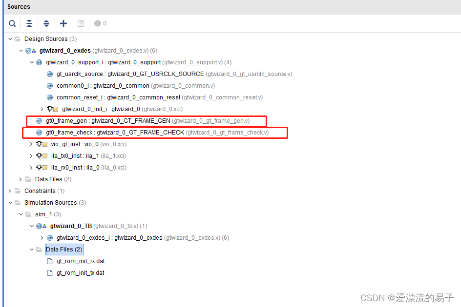
| module (in software) | corresponds English -ity, -ism, -ization |
| gtwizard_0_support | Example GTX, Example Clock, Reset, Original Language, etc. |
| gtwizard_0_GT_USRCLK_SOURCE | Generate TX/RXUSRCLK to generate the reference clock. |
| gtwizard_0_common | Primary Example GTXE2_COMMON Primitive |
| gtwizard_0_common_reset | come into beinggtwizard_0_commonQPLL reset signal inside |
| gtwizard_0_GT_FRAME_GEN | The important module, the data generation module. The data generation starts with reading from the file into a 512 bit deep ROM. The data is sent out one by one from the ROM. |
| gtwizard_0_GT_FRAME_CHECK | Important module, data checking module. In the simulation TX is connected to RX on TB and the data received by RX is the data sent out by TX. Similarly first read the data from the file to ROM and compare the received data with the data in ROM to see if they are the same. Thus reporting an error. |
Here to test the data transfer. xilinx has designed incremental arrays in the file.
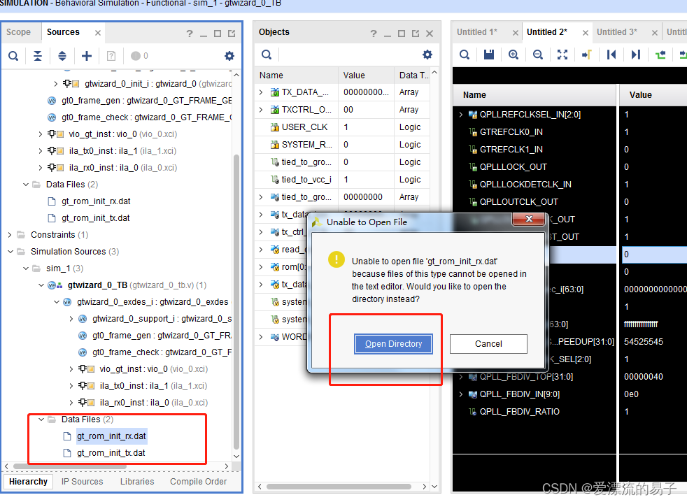
We open the file. It is found that the data sent is an incremental data.
03020100
0605047C
0A090807
…
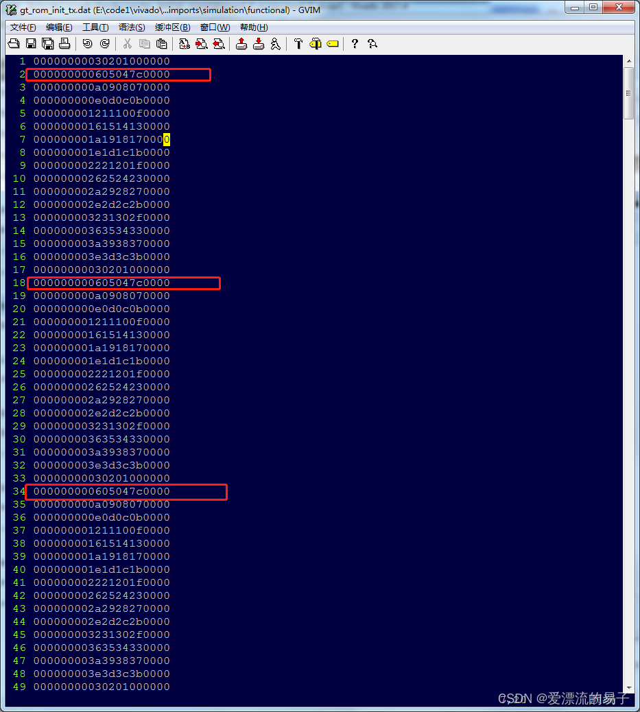
The receive data file gt_rom_init_rx.dat is consistent with the transmitter data gt_rom_init_tx.dat.
Let’s analyze the code on both the sending and receiving ends. First look at the sending side.
gtwizard_0_GT_FRAME_GEN #
    (
        .WORDS_IN_BRAM(EXAMPLE_WORDS_IN_BRAM)
    )
    gt0_frame_gen
    (
        // User Interface
        .TX_DATA_OUT ({gt0_txdata_float_i,gt0_txdata_i,gt0_txdata_float16_i}),//data to be sent
        .TXCTRL_OUT (),//Transmit port boundary alignment, not used without encoding

        // System Interface
        .USER_CLK (gt0_txusrclk2_i),//data and reset
        .SYSTEM_RESET                   (gt0_tx_system_reset_c)
);
The code on the transmitter side is simple, first read the data from gt_rom_init_tx.dat to the 512 bit deep ROM. second, accumulate read_counter_i at every clock edge to read the data from the ROM. Send it to TX.
Looking at the receiving end.
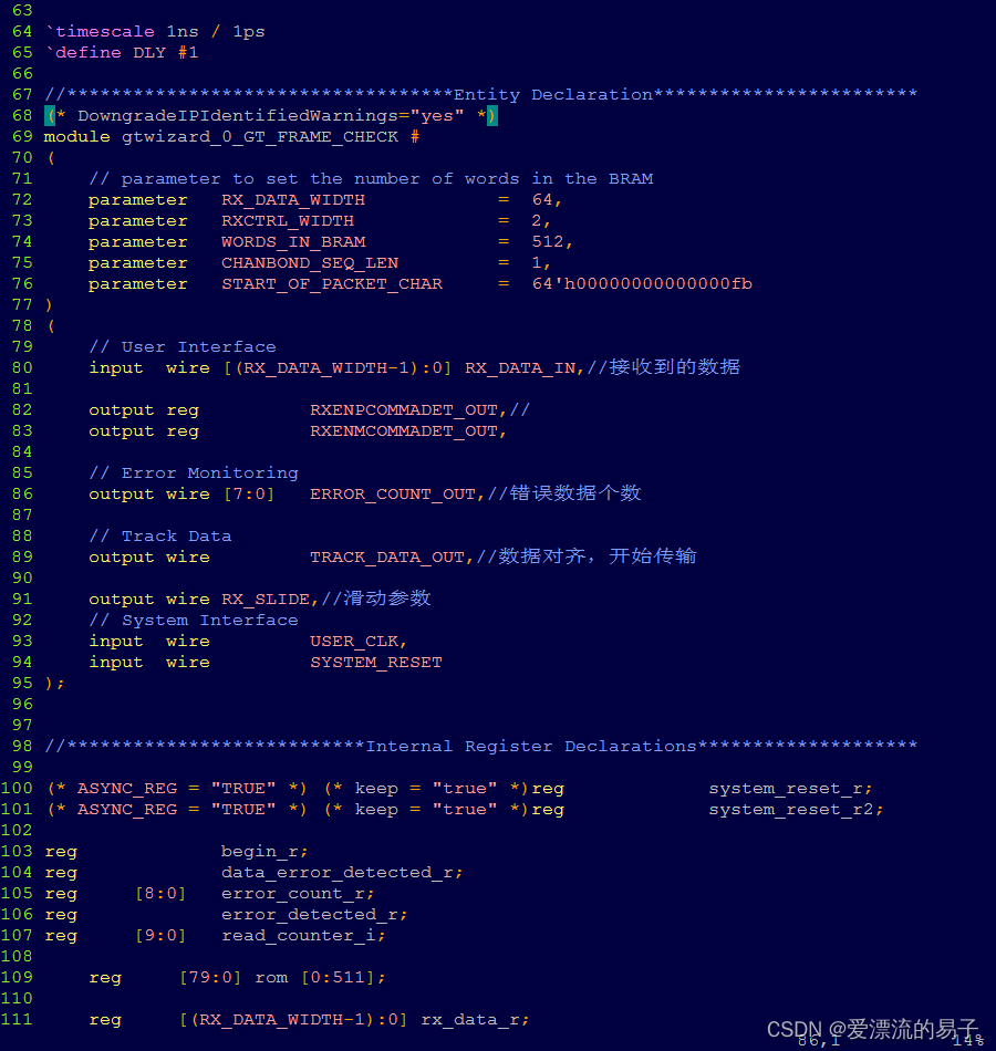
The code on the receiving side is a bit more complex compared to the sending side.
First of all the parallel data received from the receiver is not aligned. As mentioned before there is a module called RX Byte and Word Alignment for the receiver side. The alignment process can be seen in the gtwizard_0_GT_FRAME_CHECK code. It is to compare the received data with the set parameter START_OF_PACKET_CHAR to see if it is the same, if not then a RX_SLIDE is generated to make the receiver shift right once. After several right shifts, the receiver is finally aligned and receives the correct data. At this point the module will compare the received data with the data in the ROM to see if it is the same. To generate ERROR_COUNT_OUT the number of incorrect data.
    always @(posedge USER_CLK)
    begin
        if( (system_reset_r2 == 1'b1) | (rxdata_or == 1'b0) )   begin
          bit_align_r <= 1'b0;
        end else begin
            if( ({rx_data_r2[23:0],rx_data_r[31:24]} == START_OF_PACKET_CHAR) || ({rx_data_r2[15:0],rx_data_r[31:16]} == START_OF_PACKET_CHAR) || ({rx_data_r2[7:0],rx_data_r[31:8]} == START_OF_PACKET_CHAR) || (rx_data_r[31:0]== START_OF_PACKET_CHAR) )
            begin
                bit_align_r <= 1'b1;
            end
        end
    end
The TRACK_DATA_OUT signal is output next, indicating that the link is established and data can be transmitted normally. Next we modify the transmitter and receiver modules.
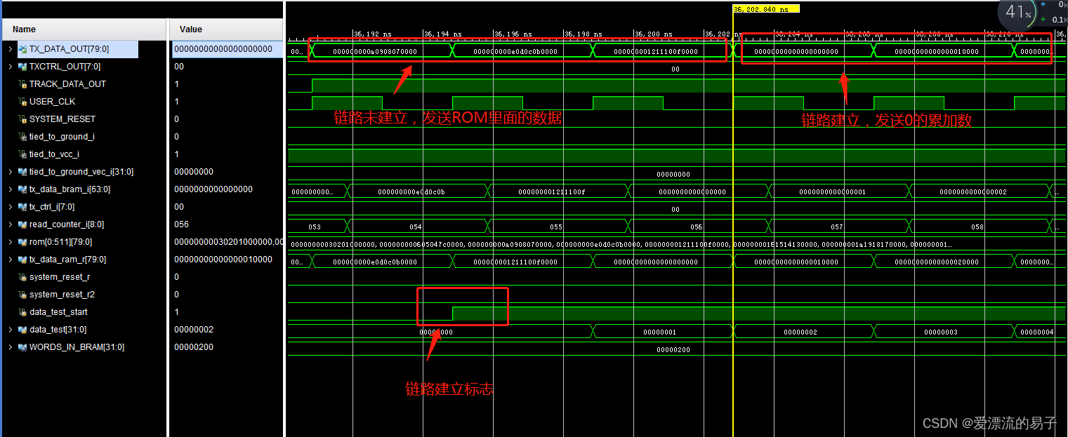
Let’s set it up in the transmitter module to be ready to send the data accumulator when the link is detected to be established, 0, 1, 2, 3, 4…
reg     data_test_start;

    // When the link is complete, it enters the data sending mode.
   always@(posedge USER_CLK)
   begin
           if(system_reset_r2)
                   data_test_start    <= 1'b0;
           else if(TRACK_DATA_OUT == 1'b1)
                   data_test_start    <= 1'b1;
           else
                   data_test_start    <= data_test_start ;
   end


    //Modify Send. Sends the data of the ROM before the link establishment is completed, and sends the cumulative number when it is completed.
    always @(posedge USER_CLK)
    begin
            if(data_test_start == 1'b0)
                    tx_data_ram_r <= `DLY rom[read_counter_i];
            else
                    tx_data_ram_r <= `DLY {32'h0,data_test,16'h0};
    end

   reg  [31:0]  data_test;

   always@(posedge USER_CLK)
   begin
           if(system_reset_r2)
                   data_test    <= 1'b0;
           else if(data_test_start == 1'b0)
                   data_test    <= 1'b0;
           else
           begin
                   if(data_test == 32'd512)
                           data_test    <= 32'h0;
                   else
                           data_test   <=  data_test  + 32'd1;
           end
   end
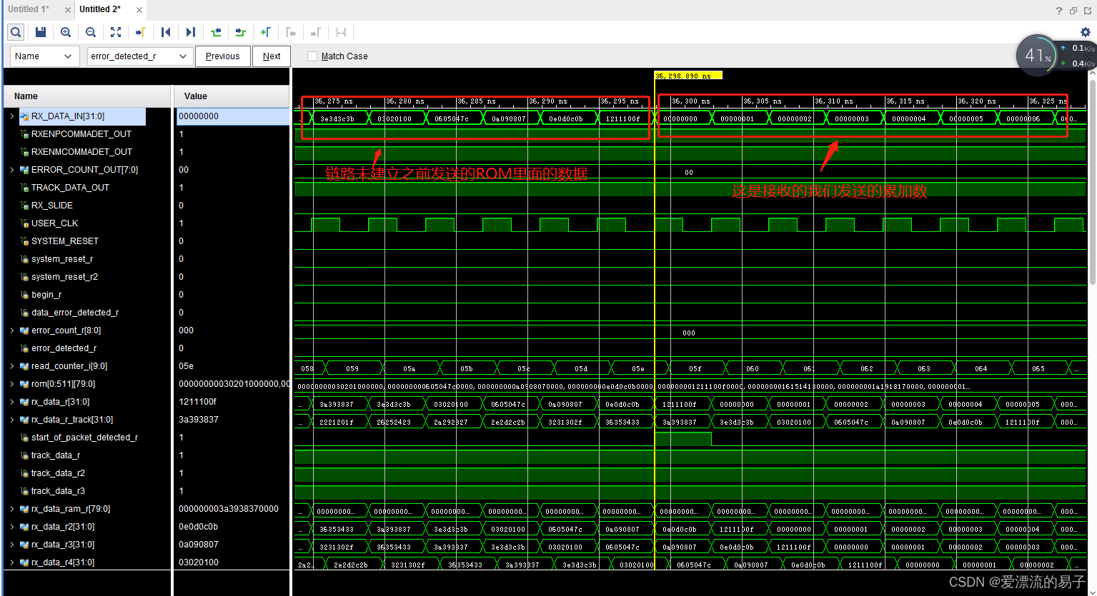
The receiver module lets him train as usual and receives data from the transmitter when the data link is established. Of course, the receiver side has not modified the check mechanism, the received data will report an error after receiving the cumulative number. But it doesn’t affect the simulation observation on our side.
Simulation modeling.
transmitter
receiving end
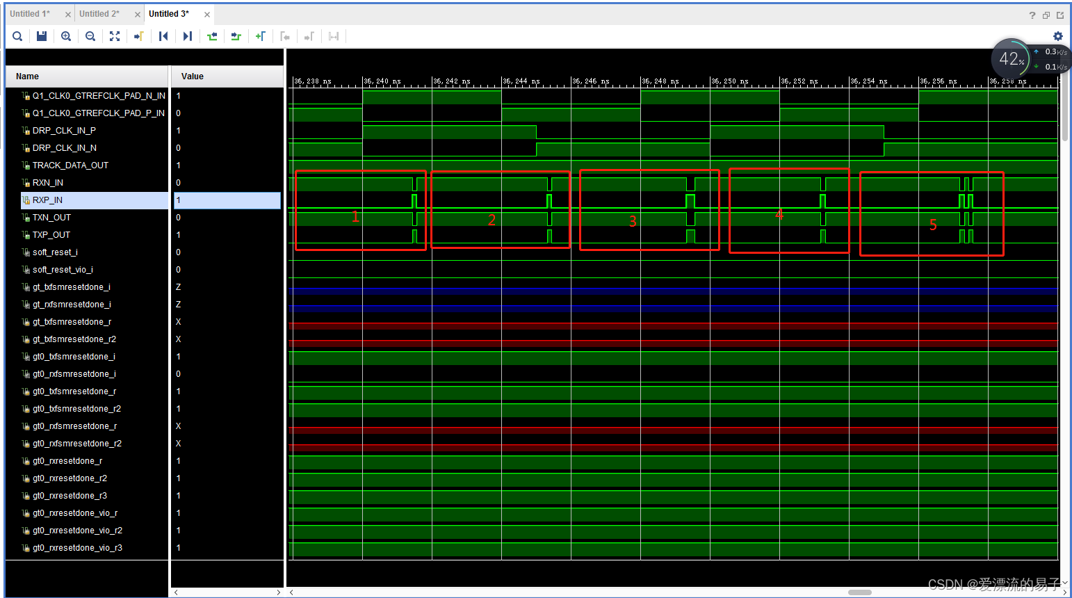
So how does the data get transmitted across TX and RX when it is not encoded?
Here we find the first five data 1, 2, 3,, 4, 5 transmitted on the serial bus, the waveforms are consistent with the waveforms of the data converted from parallel to serial. From the above, we can see that there is no coded data transmitted on the TX and RX will be a continuous high and low level, which is very unfavorable to the RX receiving end of the CDR’s data clock recovery. Of course, we are only doing simulation here, the BER test should be observed on the board in combination with the eye diagram.
-
Example project simulation using 8B/10B encoding
Mode 2: 8Gbps rate, 8B/10B encoding mode, 32-bit data bit width. rx reference clock 125MHZ.
The IP Configuration screen just needs to select 8B/10B encoding in the Encoding Mode screen. You can see that the external data bit width is still 32 bits, but the internal data bit width has become 40 bits.
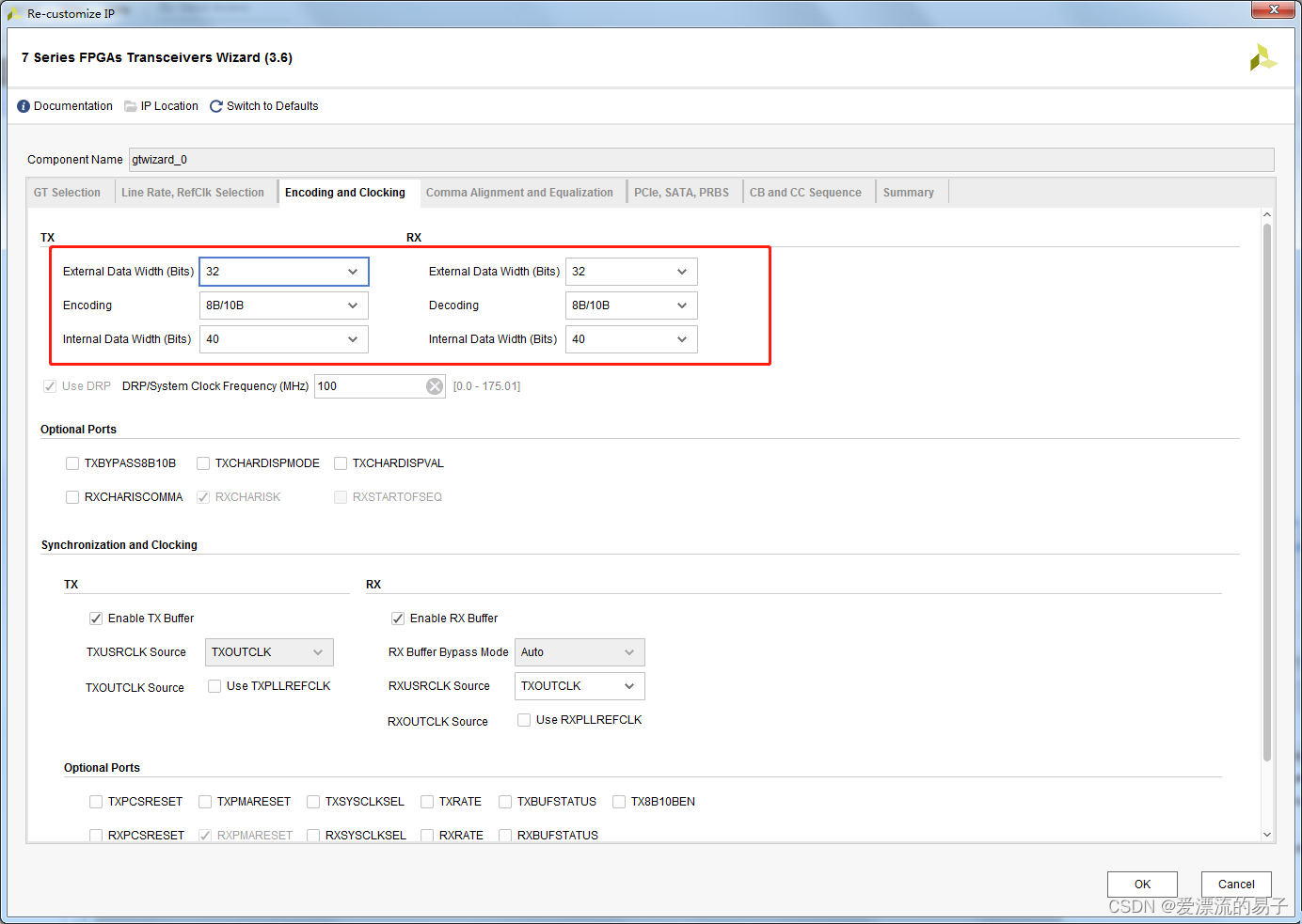
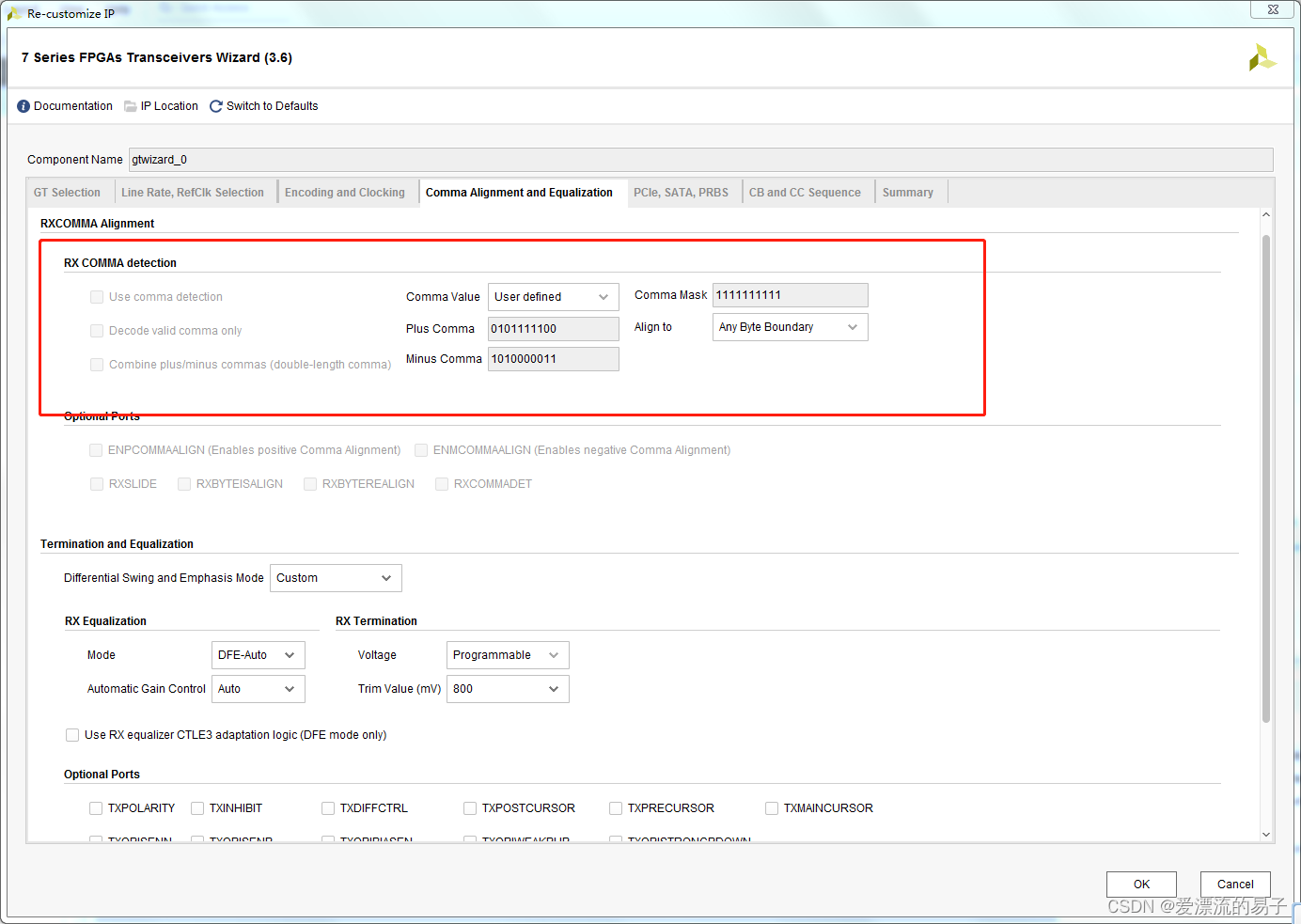
Meanwhile, the boundary alignment automatically selects K28.5, and here we just configure it by default.
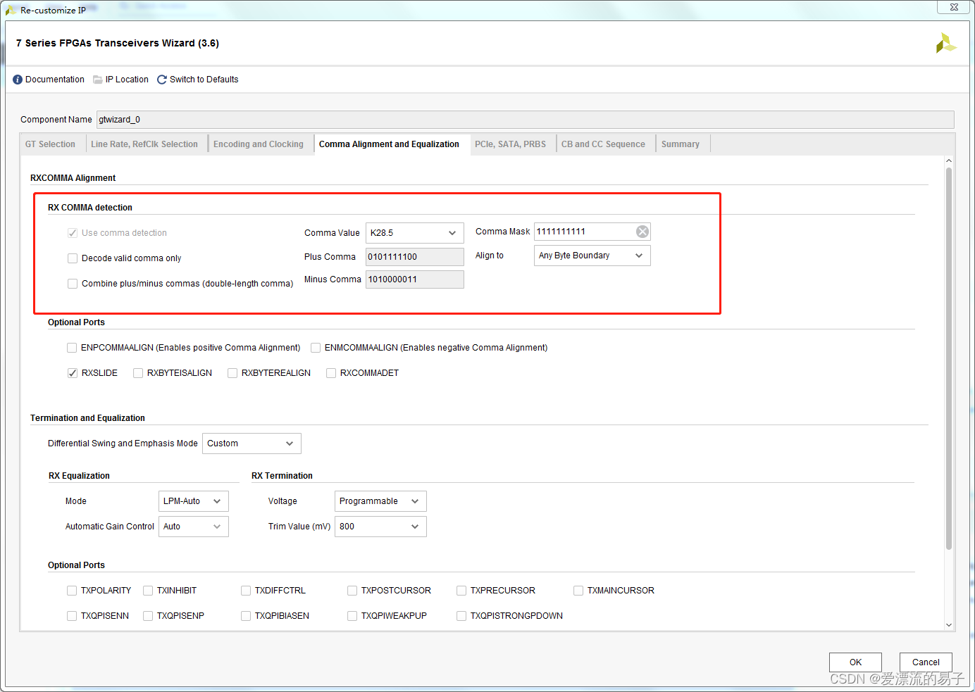
Again, let’s open example project.
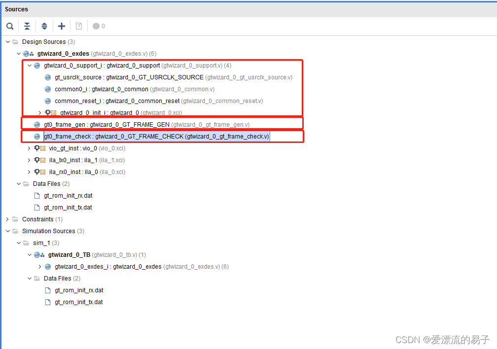
The code structure of the project does not differ from the structure in the no-code mode. There is no difference in the functionality of the individual modules, which are not described here.
Here’s a look at the send/receive data file prepared by XILINX. When you open the file, you will find that the data sent is also an incremental array.
03020100
060504BC
0A090807
…
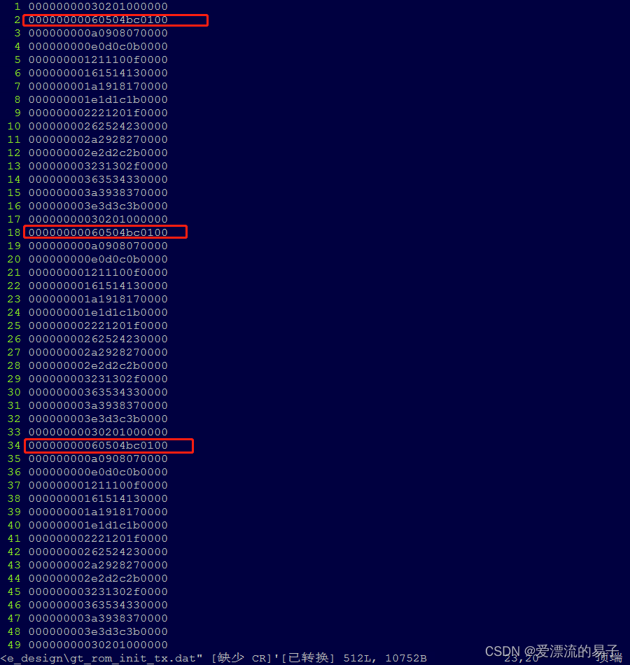
We see some strange data here, with the appearance of 00000000060504bc0100 and a 0100 in the lower sixteen bits.
Here we are talking about the 8B/10B code, so what is this code? And what’s the one thing he’s done?
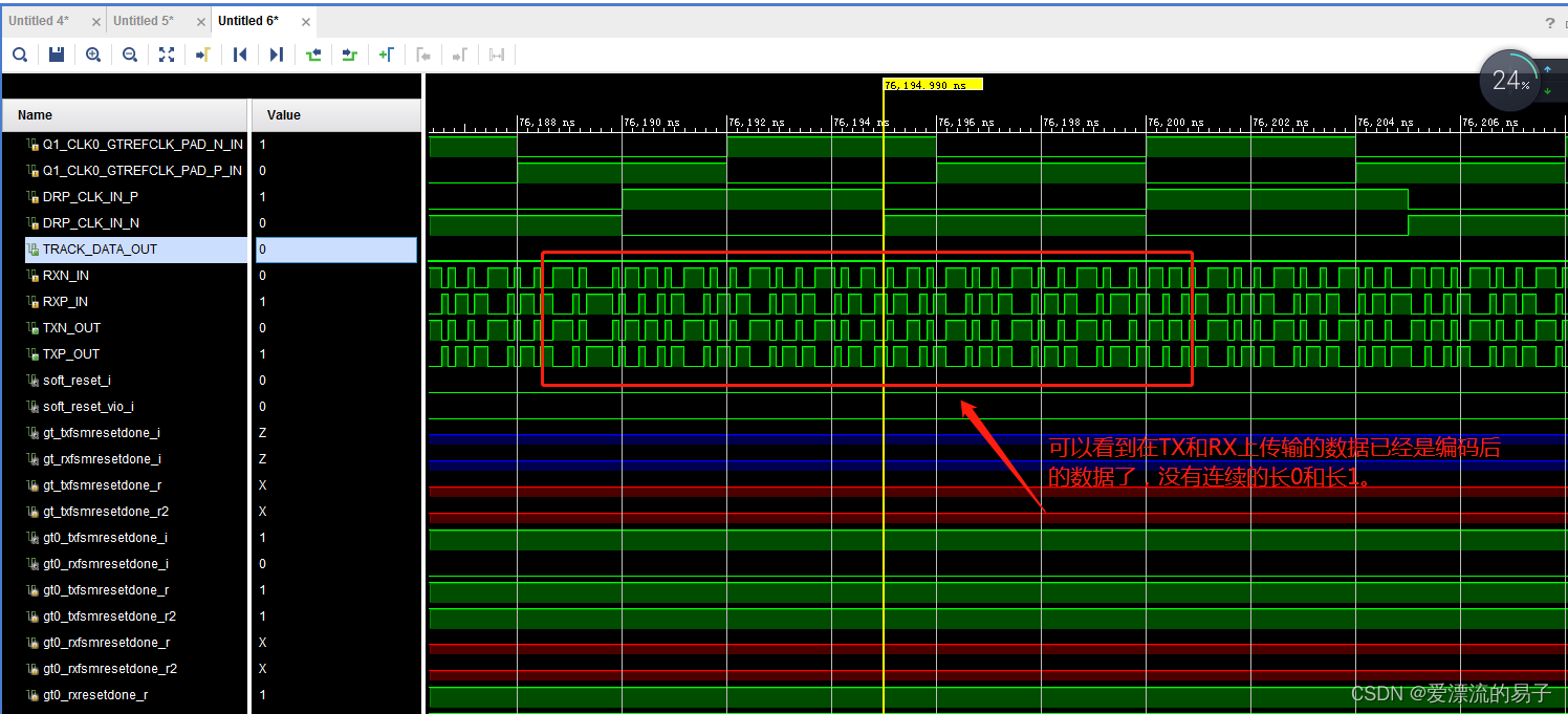
After the simulation above we see that the data that is not encoded will have a long stretch of consecutive zeros and ones after it is sent out through the TX and RX. As mentioned again earlier, the RX receiver needs toThe recovered clock and data are extracted from the incoming data stream. Then for data streams that do not change for long periods of time, this causes jitter in the recovered clock, which results in unanticipated miscoding. That is, transmission errors. This is of course something we don’t want to see, so in order to reduce this BER. In order to reduce this BER, and to enable the CDR to recover a stable clock, it is necessary to use an encoder. The data to be sent is encoded. So that the transmitted data is balanced with zeros and ones and has a variation of zeros and ones (reducing the occurrence of consecutive zeros and ones).
I won’t go deeper here for space reasons.
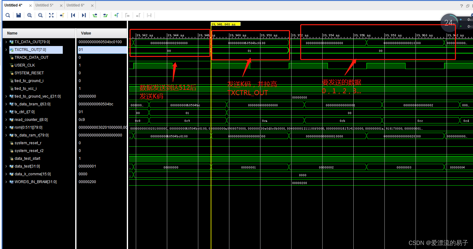
XILINX’s SERDES uses 8B/10B encoding to transmit data messages. And special characters (K characters) are used for control functions.The TXCHARRISK port is used to indicate whether the data on the TXDATA is K-code or data.The 8B/10B encoder checks to see if the received TXDATA byte matches any of the K-codes, and if it does, then it pulls the TXCHARRISK high.
Similarly, on the receive side, the 8B/10B decoder, when RXDATA detects a K-code, the decoder will drive RXCHARISK high.
Again, let’s modify the module a bit to send our customized data instead.
// When the link is complete, it enters the data sending mode.
   always@(posedge USER_CLK)
   begin
           if(system_reset_r2)
                   data_test_start    <= 1'b0;
           else if(TRACK_DATA_OUT == 1'b1)
                   data_test_start    <= 1'b1;
           else
                   data_test_start    <= data_test_start ;
   end


    //Modify Send. Sends the data of the ROM before the link establishment is completed, and sends the cumulative number when it is completed.
    always @(posedge USER_CLK)
    begin
            if(data_test_start == 1'b0)
                    tx_data_ram_r <= `DLY rom[read_counter_i];
            else
                    tx_data_ram_r <= `DLY {32'h0,data_test,data_k_comme};
    end

   reg  [31:0]  data_test;
   reg  [15:0]  data_k_comme;

   always@(posedge USER_CLK)
   begin
           if(system_reset_r2)
           begin
                   data_test    <= 32'h0;
                   data_k_comme <= 16'h0;
           end
           else if(data_test_start == 1'b0)
           begin
                   data_test    <= 1'b0;
                   data_k_comme <= 16'h0;
           end
           else
           begin
                   if(data_test == 32'd512)
                   begin
                           data_test    <= 32'h060504bc;
                           data_k_comme <= 16'h0100;
                   end
                   else if(data_test == 32'h060504bc)
                   begin
                           data_test    <= 32'h0;
                           data_k_comme <= 16'h0;
                   end
                   else
                   begin
                           data_test   <=  data_test  + 32'd1;
                           data_k_comme <= 16'h0;
                   end
           end
   end
Similarly we prepare the data we want to send on the TX after the link is completed. The data class to be sent is allowed to be a data loop from 0 to 512, sending the K-code once after a loop is completed. And recount.
Similarly, in the receiving module. The receiving module will judge the received data. We need to not change the exchange of data bits after reception after the first judgment. We change the SEL judgment to not reset the value of SEL after receiving data different from ROM.
    // Comma realignment logic might be needed. 4 levels of registering for RXDATA to meet timing
    // In 4 Byte scenario, when align_comma_word=1, Comma can appear on any of the four bytes.
    // { BYTE3 | BYTE2 | BYTE1 | BYTE0 } - Comma can appear on BYTE0/1/2/3
    // If Comma appears on BYTE1/2/3, RX_DATA is realigned so that Comma appears on BYTE0 in rx_data_r_track
    always @(posedge USER_CLK)
    begin
//        if(reset_on_error_in_r2 || system_reset_r2)    sel <= 2'b00;
        if( system_reset_r2)    sel <= 2'b00;
        else if (begin_r && !rx_chanbond_seq_r)
        begin
            // if Comma appears on BYTE3 ..
            if((rx_data_r[(RX_DATA_WIDTH - 1) : 3*RX_DATA_WIDTH/4] == START_OF_PACKET_CHAR[7:0]) && rxctrl_r[3])
                sel <= 2'b11;
            // if Comma appears on BYTE2 ..
            else if((rx_data_r[(3*RX_DATA_WIDTH/4 - 1):2*RX_DATA_WIDTH/4] == START_OF_PACKET_CHAR[7:0]) && rxctrl_r[2])
            begin
                sel <= 2'b10;
            end
            // if Comma appears on BYTE1 ..
            else if((rx_data_r[(2*RX_DATA_WIDTH/4 - 1):RX_DATA_WIDTH/4] == START_OF_PACKET_CHAR[7:0]) && rxctrl_r[1])
            begin
                sel <= 2'b01;
            end
            // if Comma appears on BYTE0 ..
            else if((rx_data_r[(RX_DATA_WIDTH/4 - 1):0] == START_OF_PACKET_CHAR[7:0]) && rxctrl_r[0])
            begin
                sel <= 2'b00;
            end
        end
end
This way we are observing the simulation of the sending module.
Similarly we observe the simulation of the receiver module.
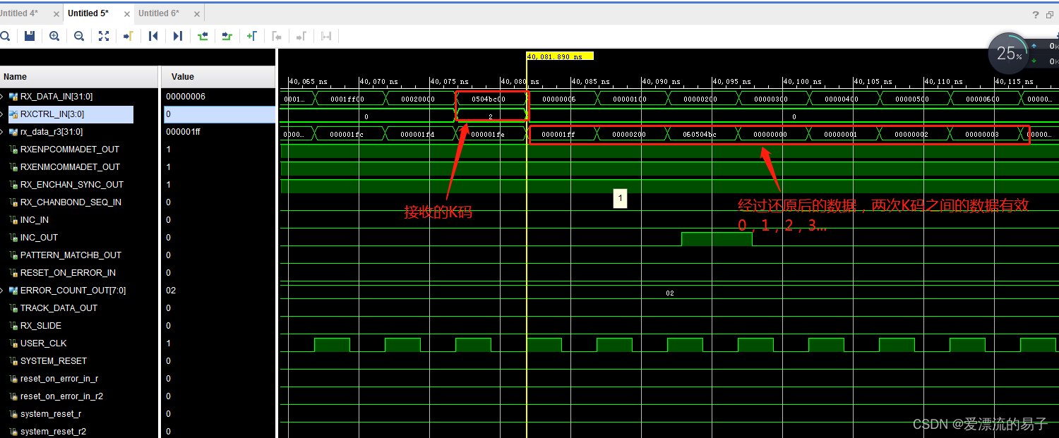
Similarly observe the effect of data transfer on TX and RX.
-
Example project simulation using 64B/66B encoding
Previously, we looked at the modes of transmission of SERDES with no encoding and with 8B/10B encoding. However, for many high-speed protocols, 64B/66B encoding is used, which reduces the encoding overhead compared to 8/10B encoding.
Let’s take a look at it on IP below.
Similarly, we select 64B/66B encoding on IP and then open the example project. the configuration interface is as follows, when selecting 64B/66B encoding, he has two modes, one is external counter and the other is internal counter. The two modes of the project XILINX are set up in the example project. Here we directly choose 64B/66B with int Seq Ctr mode.
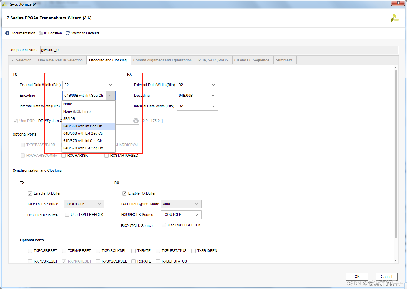
Since 64B/66B encoding is selected, comma is not needed. The default is not used.
Again, let’s open the example project directly. The structure of the code after opening the project is as follows. There are two more modules compared to the uncoded and 8B/10B coding modes. These are scrambler and descrambler specific to 64B/66B coding mode.
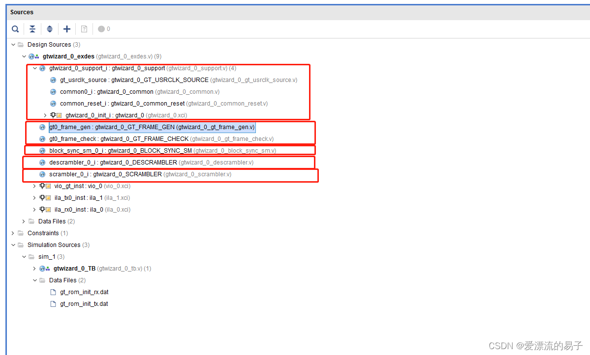
| module (in software) | corresponds English -ity, -ism, -ization |
| gtwizard_0_BLOCK_SYNC_SM | Alignment module specific to 64B/66B encoding mode. Performs a lookup on the received gt0_rxheader_i header. |
| gtwizard_0_DESCRAMBLER | Descrambler in 64B/66B coding mode. The data received by the RX is descrambled and the descrambled data is detected before entering the gtwizard_0_GT_FRAME_CHECK module. |
| gtwizard_0_SCRAMBLER | Scrambler in 64B/66B coding mode. |
Then to use 64B/66B encoding, you need to understand the basic information of this encoding. 64B/66B encoding encodes 64bit data or control information into 66bit blocks for transmission. the first two digits of the 66bit block indicate the synchronization header, which is mainly used for the alignment of the data at the receiving end and the synchronization of the combined data stream. There are two kinds of header, 01 and 10, 01 means that the 64bit behind are all data, 10 means that the 64bit behind are a mixture of data and control signals. And code wrap is a way to rearrange or encode the data to make the division of 0 and 1 in the data more randomized, thus improving the stability of communication.
Here the scrambling and descrambling code XILINX have been given out, we will not go too much research. Let’s focus on the data sending and data receiving modules. How to add the right code to send your own data on this example project.
The same XILINX also sets up test data for data transfer here. Let’s take a look at his test data.
The data tested were
00000000000000fb0100
00000000030201000000
00000000070605040000
…
incremental data, and each fifteen data will produce a00000000000000fb0100Used to generate the header.
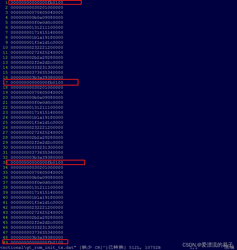
Next, let’s modify the module a bit to send our customized data instead. First the data link is established and the customized data is generated. Note that the data is in counter operating mode and there is a time pause for the data to be sent. That is, if TXDATAVALID_IN is equal to one we update and send the data as it is about to occur. In the case of zero we pause the data sending (i.e. latch)
// When the link is complete, it enters the data sending mode.
   reg     data_test_start;

   always@(posedge USER_CLK)
   begin
           if(system_reset_r2)
                   data_test_start    <= 1'b0;
           else if(TRACK_DATA_OUT == 1'b1)
                   data_test_start    <= 1'b1;
           else
                   data_test_start    <= data_test_start ;
   end


    //Modify Send. Sends the data of the ROM before the link establishment is completed, and sends the cumulative number when it is completed.
    always @(posedge USER_CLK)
    begin
            if(data_test_start == 1'b0)
                    tx_data_ram_r <= `DLY rom[read_counter_i];
            else
                    tx_data_ram_r <= `DLY {32'h0,data_test,data_k_comme};
    end

   reg  [31:0]  data_test;
   reg  [15:0]  data_k_comme;

   always@(posedge USER_CLK)
   begin
           if(system_reset_r2)
           begin
                   data_test    <= 32'h0;
                   data_k_comme <= 16'h0;
           end
           else if(data_test_start == 1'b0)
           begin
                   data_test    <= 1'b0;
                   data_k_comme <= 16'h0;
           end
           else if(TXDATAVALID_IN == 1'b1)
           begin
                   if(data_test == 32'd200)
                   begin
                           data_test    <= 32'h0000_00fb;
                           data_k_comme <= 16'h0100;
                   end
                   else if(data_test == 32'h0000_00fb)
                   begin
                           data_test    <= 32'h0;
                           data_k_comme <= 16'h0;
                   end
                   else
                   begin
                           data_test   <=  data_test  + 32'd1;
                           data_k_comme <= 16'h0;
                   end
           end
   end
The same is not modified on the receiving end. The data received this way generates an ERROR_COUNT_OUT error, but this is in comparison to the customized data inside the ROM. The data we normally transmit is still correct.
This way we are observing the simulation of the sending module.
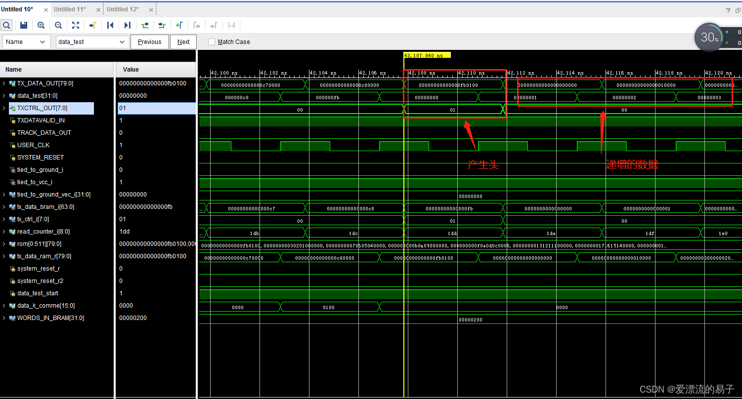
Stop updating data if TXDATAVALID_IN is zero.

In this way we are observing the simulation of the receiver module. The received data stops updating when RXDATAVALID_IN is zero. And the received data is a continuous incremental array from 0 to 200.

